AI’s energy hunger just hit a turning point.
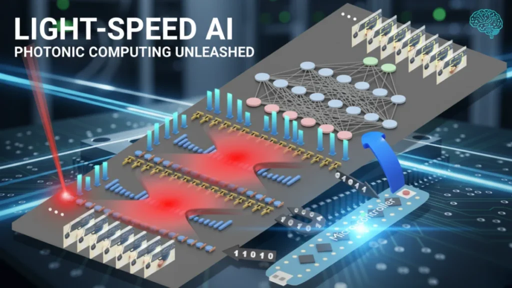
A team at the University of Florida has unveiled a silicon chip that uses light, not just electricity, to power one of AI’s most demanding computations — a move that could make machine learning 100 times more efficient.
Key Takeaways
- New chip uses laser light to perform AI computations.
- Achieves near-zero energy convolution operations.
- Maintains 98% accuracy in neural network tests.
- Could cut AI’s rising electricity demand dramatically.
- Opens path for faster, greener machine learning chips.
Researchers at the University of Florida have created a silicon chip that uses light, rather than electricity, to run convolution operations in AI. This innovation makes neural network processing up to 100 times more efficient while keeping accuracy at 98%. It could help cut AI’s soaring energy costs and enable faster, sustainable computing.
Why This Matters
Artificial intelligence is growing at breakneck speed, but the trade-off has been staggering energy consumption. From data centers powering language models to GPUs crunching image recognition, the electricity bill is rising. A newly developed chip could flip that script by weaving light directly into AI computation.
How the Chip Works
The chip, built at the University of Florida and detailed in Advanced Photonics, is designed for convolution operations — the pattern-recognition step at the heart of AI. Instead of processing with electrons alone, it converts data into laser light.
That light passes through microscopic Fresnel lenses etched into the silicon, executes the math, and then converts back to digital signals. The result: near-zero energy use and blistering speed.
A Leap in Efficiency
Early tests show the prototype chip classifying handwritten digits with 98% accuracy — on par with traditional processors. But the energy difference is striking: computations run up to 100 times more efficiently than on conventional silicon, researchers say (SPIE, 2025).
Expert Insights
“Performing a key machine learning computation at near zero energy is a leap forward for future AI systems,” said Volker J. Sorger, the Rhines Endowed Professor in Semiconductor Photonics at UF. “This is critical to keep scaling up AI capabilities in years to come.”
Co-author Hangbo Yang emphasized another edge: wavelength multiplexing. By running multiple colors of light through the same chip, researchers can process several data streams simultaneously — a feature electronic chips can’t easily replicate.
Industry Implications
AI chipmakers from NVIDIA to AMD are already experimenting with optical components. Integrating full optical convolution units could open the door to consumer and enterprise chips that consume a fraction of today’s energy. That’s a big deal for hyperscalers like Google, Amazon, and Microsoft, all of which spend billions annually on electricity for AI training.
The Bigger Picture
The timing couldn’t be more urgent. AI models like GPT-4 and beyond require tens of thousands of GPUs, consuming the power equivalent of small cities. Scaling to trillion-parameter models could become unsustainable without efficiency gains.
If adopted broadly, chips like UF’s design could reduce both the carbon footprint and operating costs of AI. That aligns with growing pressure on the industry to meet sustainability targets.
What Happens Next
The prototype is still early-stage, but researchers say integration is feasible since the lenses are fabricated with standard semiconductor techniques. Collaborations with UCLA, George Washington University, and the Florida Semiconductor Institute suggest commercial pathways are already being explored.
Sorger predicts that “chip-based optics will become a key part of every AI chip we use daily” within the next decade.
Conclusion
This isn’t just a lab demo — it’s a signal of where AI hardware is heading. By merging optics and silicon, the industry may finally get a way to expand AI power without blowing up the electric grid.
Source: SPIE-International Society for Optics and Photonics
